# Load Switch
Charge controllers are often equipped with a load switch that disconnects consumers and protects the battery from deep-discharge. If supported by the charge controller, the load switch can also be used for advanced control of connected loads, e.g. switching on lights during the night.
The following image shows the layout of a typical MPPT charge controller with the DC/DC power stage between the solar panel and the battery and a switch between the battery and the load output.

Even though it might seem very simple to switch on and off a load using a MOSFET, a reliable load switch control can get quite complicated. The load switch needs to protect itself and the charge controller from overcurrents and from exceeding its thermal limits. In addition to that, it must protect the wires from short circuits, acting like an electronic fuse. These different protection features are described below in more detail.
# High-side vs. low-side
When switching off an electrical load, there are basically two ways to disconnect its power, either at the positive terminal (high-side) or the negative terminal (low-side).
Switching the low-side is the most easy method from electrical perspective. An N-channel MOSFET can be used, driven by an existing positive supply voltage, e.g. the battery itself. On the high-side, an N-channel MOSFET needs a drive voltage at the gate that is above the battery voltage. This requires additional circuitry like a charge pump.
As an alternative, a P-channel MOSFET can be used to switch the high-side. However, P-channel MOSFETs are more expensive and feature a higher on-state resistance compared to N-channel MOSFETs.
In most cases it is more safe to use high-side switching in order to prevent additional ground paths which could either make the switch ineffective or even lead to damage in other parts or wires.
Fig. 2 shows a typical scenario where the use of low-side switches is problematic.

If two devices powered via different paths from a single source (the 12V battery in this case) are connected via a second path like audio, video or USB interfaces, these interfaces provide a redundant ground path. If one of the consumers (e.g. the screen) is switched off via the negative terminal, the current will flow back to the battery via the small signal wire. This does not only create issues with the signal transmission or makes the switch ineffective. It could also overheat or destroy the signal wire due to excessive current.
In a car or a boat, the chassis or hull is typically connected to the negative terminal of the battery (meaning it is "grounded"). This could provide the undesired second ground path in case of a short circuit. With a ground path via the chassis the switch would not have any effect anymore.
# Inrush current during turn-on
A load with high capacitance will generate an inrush current after the switch was turned on. This current spike can be limited with two different methods:
# Slew-rate limitation using gate capacitor
This approach is described in the Application Note AND9093-D (opens new window) by ON Semiconductors. Also this page (opens new window) by ROHM gives a short introduction to the topic.
# PWM switching
Instead of switching on continuously, a PWM signal can be applied to the load switch, so that the capacitance is charged in several small quantities over a few milliseconds. Depending on the PWM frequency, this method requires stronger MOSFET gate drivers.
This method is also described in detail in the following blog post (opens new window) by Victron Energy.
# Overcurrent
The maximum continuous current the load switch can handle is mainly determined by the thermal limits of the MOSFET. The relevant temperature is the junction temperature which has to stay below the maximum temperature stated in the datasheet. Typical values are around 150 °C.
# Thermal model
As the junction temperature cannot be measured directly, the following thermal model provides a method to estimate it based on the measured current flow and control the load switch accordingly.
The heat flow dissipated in the MOSFET is calculated from its on-state resistance and the current going through it:
For simplicity reasons, the on-state resistance is assumed to be independent of the temperature, so the worst case resistance should be considered for a safe estimation.
The dissipated heat is partly stored in the thermal capacity of the MOSFET and its surrounding PCB area, considered as a single thermal mass . Another part of the heat is transferred to the ambient, described by the thermal resistance between junction and ambient, .
Using an energy balance, the junction temperature at a time step can be calculated based on the temperature of the previous step , the ambient temperature and the average heat dissipated during the period between two steps:
With the thermal time constant of the system the equation can be rewritten as:
The time constant depends on the PCB design, the used components and attached heat sinks. It is normally quite small, in the order of a few seconds. It can be determined from a measured temperature response after a load step or estimated based on experience with similar designs.
As the circuit should be designed for a certain maximum constant current at a maximum expected ambient temperature , the steady-state thermal resistance can be expressed as:
The maximum junction temperature for the layout should be chosen with some safety margin to the value specified in the datasheet.
This leads to the final temperature model equation:
For the implementation in the microcontroller, the previous temperature has to be stored, with a starting condition equal to the ambient temperature . is the time between each call of the function and is the measured current through the MOSFET. The other values are constant for a given design and can be determined during testing.
# Short circuit
Normally, there should be a fuse installed at the battery terminal to protect the wires from short circuits, which also protects the load output. However, even if the fuse rating at the battery is not much higher than the rating of the load output, fuses react quite slow. Typical automotive blade fuses (opens new window) for example need more than 10 ms to melt even for approx. 10x the rated current.
MOSFET datasheets normally state a so-called safe operating area, which shows the maximum allowed current vs. the drain-source-voltage. The following example is from the Nexperia PSMN5R2-60YL datasheet (opens new window):
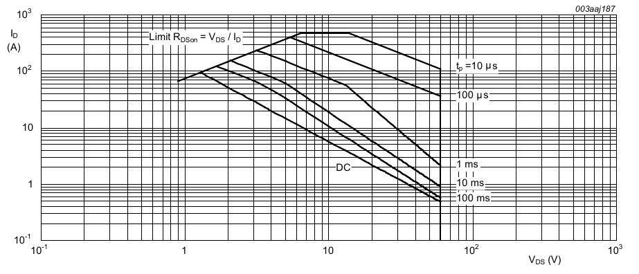
As long as the maximum junction temperature is not exceeded, this MOSFET can handle 100A continuously. However, under real operating conditions with passive cooling via the PCB, the continuous current will be in the range of 20A. During a short-circuit, the current rises very quickly, only limited by the impedance of the battery, the wires and the PCB.
According to this study (opens new window), a dead short circuit of VRLA lead-acid batteries in the range of 100 Ah can reach currents >2000 A within less than 10 ms. So the MOSFET could get destroyed before any fuse reacted.
# Inrush current when connecting capacitive loads
It would be a simple task to just switch off immediately as soon as a current above a certain limit is reached. However, this sort of protection creates false positives when connecting a load with a high input capacitance. A capacitance acts as a short circuit in the short moment of connection, but the current decreases quickly after the capacitor got charged.
The following simplified RLC circuit can be used to analyze the behavior of the system:

The resistance consists of the battery internal resistance, the wire resistance and any resistance inside the charge controller, e.g. because of connectors or a shunt for current measurement.
The wire inductance slows down the current increase and reduces the current peak during a failure. So the worst case is a short wire. The self-inductance of two parallel wires (opens new window) with a conductor radius , a distance between the conductors and a length of the pair is:
This results in an inductance of approx. 1 µH per meter for a pair of 4 mm² wires.
The following interactive graph shows the current vs. time with worst-case assumptions as default values:
- Total wire length of 1 m (calculations assume 4 mm² cross-section)
- A good quality large VRLA battery (opens new window) at full state of charge with 5 mΩ internal resistance plus another 5 mΩ contributed by the charge controller terminals and PCB.
- A low-ESR electrolytic capacitor of 1000 µF with around 20 mΩ ESR (e.g. Panasonic FR series)
The default values are realistic for what a typical 10-20A charge controller needs to detect and handle. In order to protect the MOSFET, the charge controller should switch off within less than 20 µs in case of the steep current increase of the short circuit. You can change the values to get an impression of your particular system and the general influencing factors on the maximum current.
# Digital solution with fast ADC
In order to distinguish between inrush current for capacitive loads and an actual short circuit, the microcontroller has to take multiple measurements and not only consider the absolute values, but also the slope of the current.
For a fast detection of the steep short circuit current increase, a sample frequency of less than 5 µs is necessary. This is at the limit of what lower end microcontrollers can do, if the ADC needs to measure not only the current, but also other values continuously. In addition to that, the delay and bandwidth of the current measurement have to be considered.
# Analog solution with filter and comparator
A comparator can be used to trigger a load switch-off signal as soon as a certain threshold of the current measurement signal is reached. As the comparator does not consider the slope or the length of the pulse, but just the absolute value, this approach can lead to false positives as described above if the signal is not filtered.
The current measurement output normally contains a low-pass filter (RC circuit). The filter time constant should be chosen such that the maximum allowed pulse caused by a capacitor just does not yet trigger the comparator, i.e. the damping at the frequency of the pulse is high enough to get an output signal below the threshold. In order to validate the correct filter layout, SPICE simulation of the circuit and laboratory tests should be used.
The comparator can be a dedicated part on the PCB that pulls down the MOSFET gate and switches the load output off. If the used microcontroller has an internal comparator, this can be used to trigger an interrupt and switch off the load output via software. In some MCUs, the comparator can also directly control an output pin without any interference of software.
The approach using an internal comparator to drive a GPIO pin is used in the Libre Solar PWM charge controller (see hardware (opens new window) and firmware (opens new window)).
# Overvoltage
If the battery voltage rises above allowed limits, e.g. because of a fault in the charger or because of transients, the load output should be switched off to protect connected consumers from overvoltage. This is a trivial task and will work reliably as long as there is enough margin to the maximum of the MOSFET.
However, switching off an inductive load like a motor or a relay can result in voltage peaks at the load switch. This is the reason why most charge controllers don't allow switching inductive loads at the load port.
In order to allow the current to decay slowly, a free-wheeling diode can be added to the load output. Such a circuit is shown in the following schematic:

A freewheeling diode in the charge controller should only be seen as an additional protection measure. Ideally, the diode should be located as close to the load itself as possible.