# Printed Circuit Board
A printed circuit board (PCB) is a carrier for electronic components. It serves for mechanical fastening and electrical connection. Almost every electronics device contains one or more printed circuit boards.
When a printed circuit board is assembled with electronics parts, the term PCB assembly (PCBA) is used:
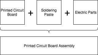
The first step to build up the hardware is ordering a PCB. Most of the PCBs for the Libre Solar devices are too complex to be produced yourself with etching or milling processes, so the PCBs will need to be ordered from a manufacturer. This guide shows how all necessary data are obtained for the fabrication.
# Native board files
More and more PCB manufacturers accept native KiCad or Eagle board files and thus provide a very easy way to get the PCB produced. For KiCad, just upload the .kicad_pcb found in your PCB root directory and you are done.
# Gerber file export
Gerber is a standardized exchange format for PCBs, which is understood by all manufacturers and which can be exported with any PCB design software.
However, the Gerber export is a bit more complicated than providing native files and needs some correct settings. We will explain the export in KiCad.
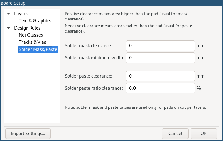
After the board is opened in Pcbnew, the solder mask clearance and min width must be set to zero. This is important because the manufacturers normally want to define the clearance themselves based on their process. Setting it to zero makes it easier for them to shrink/enlarge the pads for the solder mask. The dialogue can be found under File > Board Setup as shown in Figure 2.
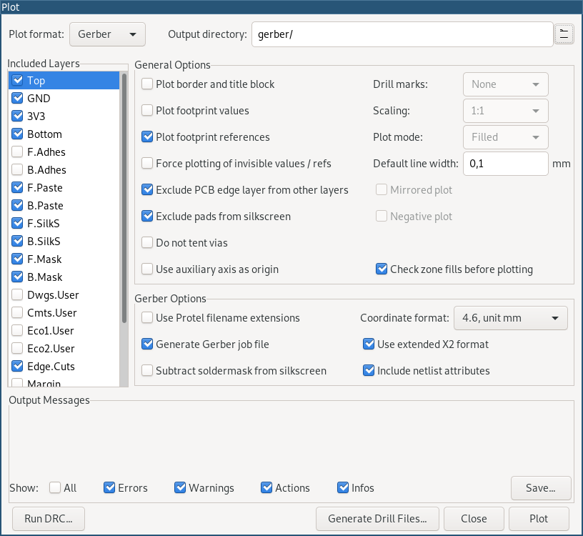
After that, open the Gerber export dialog under File > Plot and select at least the following layers for export:
- Top (Top copper plane)
- GND (Internal GND plane, if existing)
- 3V3 (Internal power supply plane, if existing)
- InX.Cu (Other internal copper planes, if existing)
- Bottom (Bottom copper plane)
- F.Silk (Front silk screen: white plots with part names, etc.)
- B.Silk (Bottom silk screen)
- F.Mask (Front solder mask: inverted surface areas for the typical green paint on the PCB)
- B.Mask (Bottom solder mask)
- Edge.Cuts (Margins along which the PCB edges should be cut, e.g. by milling)
- F.Fab (Information for parts placement on top layer)
- B.Fab (Information for parts placement on bottom layer)
Select a folder where your files should be saved and press Plot:
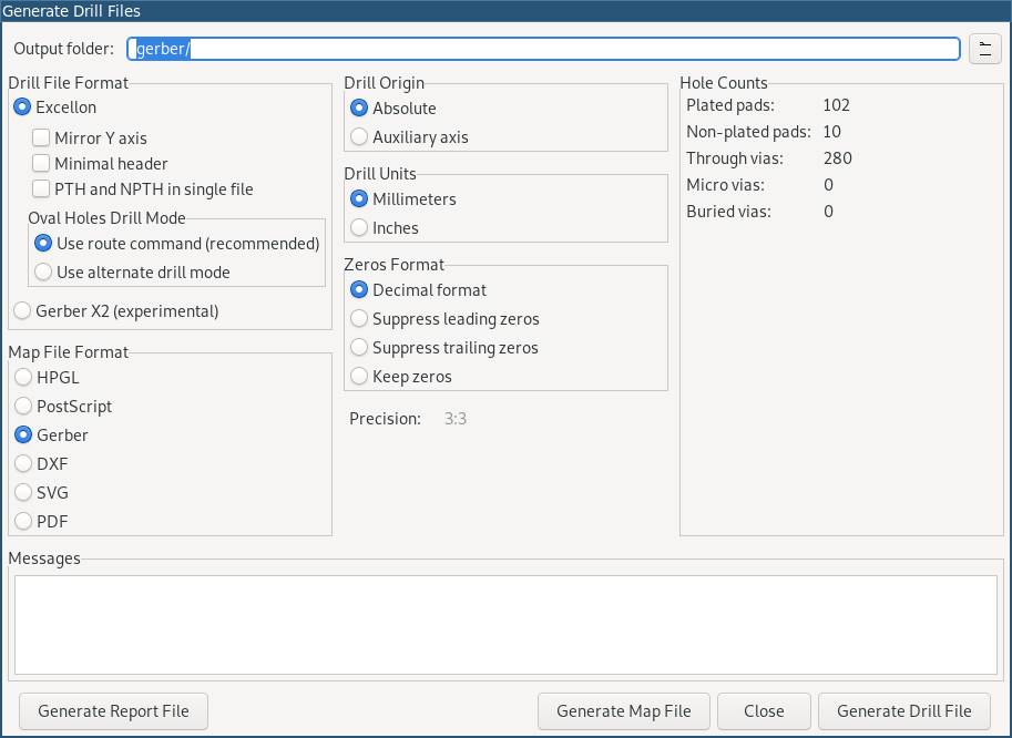
After sucessful export, press Generate Drill Files. Then select the same output directory and make sure that PTH and NPTH in single file is not checked. Otherwise, your manufacturer doesn't know which holes are copper plated or not.
After that you should have all necessary files ready for the PCB production. Compress all the files (gerber and drill files) to a .zip file and send them to the manufacturer.
Stencil →