# SMD soldering
As the name suggests, surface mount devices (SMD) are placed on the surface of the PCB, so there is no hole necessary to fix them.
The typical method for soldering SMD parts is to use solder paste and a reflow oven. However, for one-off prototypes it is also possible to solder devices with a soldering iron, as long as they don't have pads at the bottom that can't be accessed with the iron.
This chapter explains the different steps for SMD soldering for very small scale production (e.g. done manually in a fablab). In industrial scale, all these steps are done with machines, of course.
# Preparation
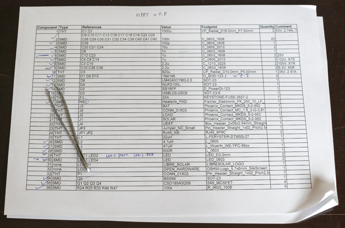
It is helpful to have the bill of materials printed out so that each placed component type can be checked, as shown in Fig. 1.
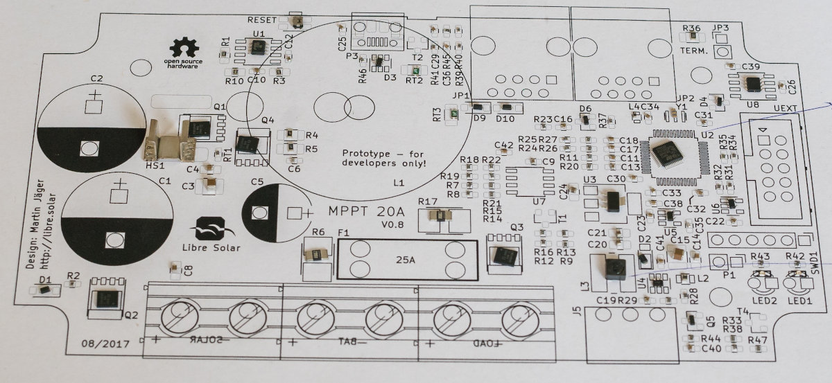
If only one or two PCBs should be soldered, the enlarged PCB silk screen and pad layers can be printed out and all components can be put in the right location prior to solder paste application, as shown in Fig. 2. This method allows to place the components very quickly and prevent the solder past from drying out.
# Solder paste application
The previously manufactured stencil is used to apply solder paste to the pads for SMD parts on the PCB.
- Fix the stencil on the PCB so that it aligns well with the pads. For a manual process, this can be done with adhesive tape.
- Apply solder paste on top of the stencil
- Evenly spread the solder paste with a scraper such that every pad is coated with paste.
The entire process is shown in Video 1.
If adjacent pins are bridged with solder paste, this is not an issue in most cases. The green soldermask on the PCB prevents contact with the solder, so that the solder is pulled towards the pins once it gets liquid in the oven.
# Pick and place
The electronic components are picked up with the help of tweezers and then placed on the PCB. Especially for components where the direction is important (diodes, ICs, etc.) a magnifying lens can be used to support the placement.
Video 2 shows a time-lapse of the placement of components for an MPPT charge controller.
Once the step is completed, an inspection should be done to see if the pins are seated correctly based on the markings on the PCB.
# Reflow oven
A reflow oven is suitable for fast soldering of entire boards in one go. If not available, also a heat gun can be used to partially heat the solder.
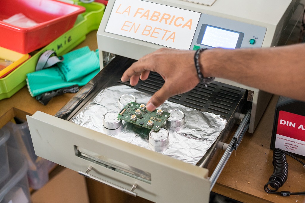
Fig. 3 shows the reflow oven available in the FabLab Fabulous St. Pauli (opens new window). It is a very common type used for small scale SMD assembly.
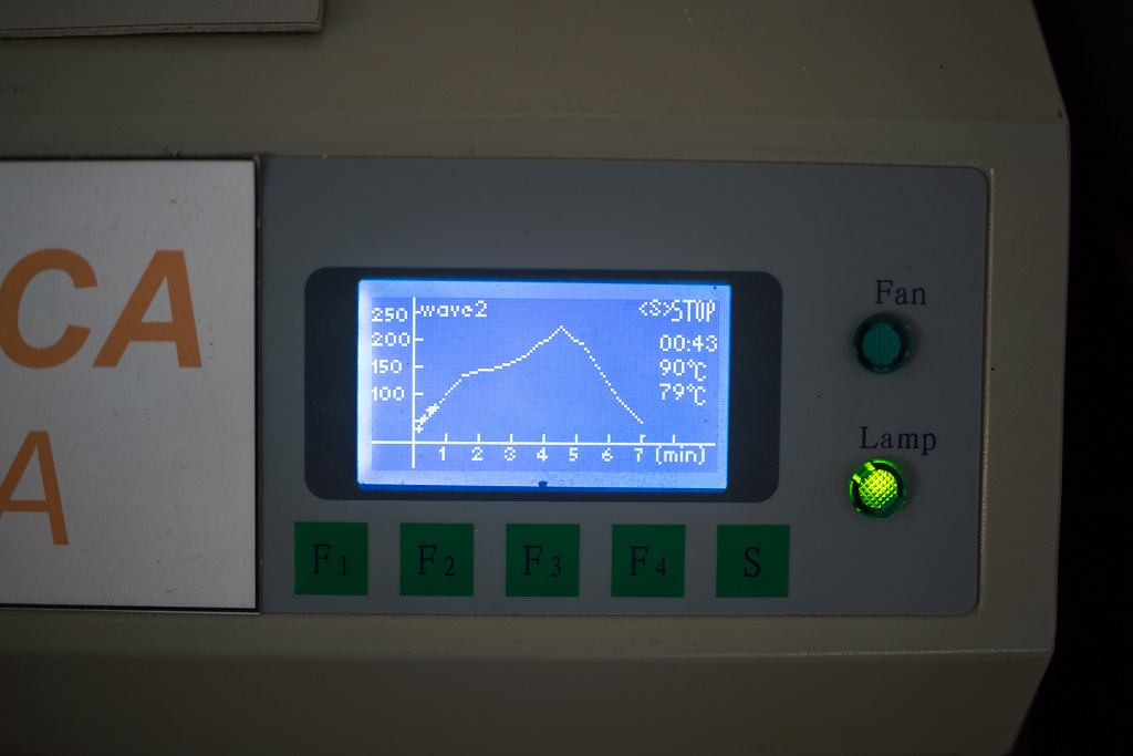
The oven has pre-programmed temperature curves which are selected based on the type of solder material and the thermal limits of the components used. The soldering process takes between 5 and 10 minutes. Fig. 4 shows the oven in progress while controlling the temperature to match the selected wave 2.
The final result after soldering is shown in Fig. 5, compared with the PCB after application of the solder paste.
← Parts Manual Check →